
Company



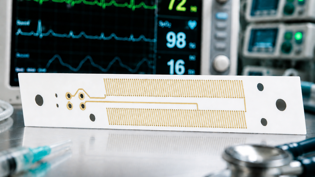
In our recent posts we covered ceramic PCB fundamentals and their role in RF and microwave hardware. Medical electronics is a different domain, but the reasons to use ceramics are consistent: electrical stability, chemical inertness, thermal performance, and the ability to build compact assemblies that hold their parameters over years or decades of service.
This post covers where ceramic microcircuits appear in medical devices, what they do there, and how we approach these applications at INCERAM.
INCERAM manufactures precision ceramic microcircuits and assemblies using thin film, thick film, and DBC metallization technologies on alumina, aluminum nitride, silicon nitride, and other advanced materials. Our product range covers ceramic sensors, microheaters, ceramic PCBs, hybrid micromodules, and power assemblies — the full range of ceramic-based components that appear at different levels of a medical device.
We are based in New Delhi, work with Indian medical device developers and manufacturers, and bring to this market decades of applied experience in ceramic microcircuit development.
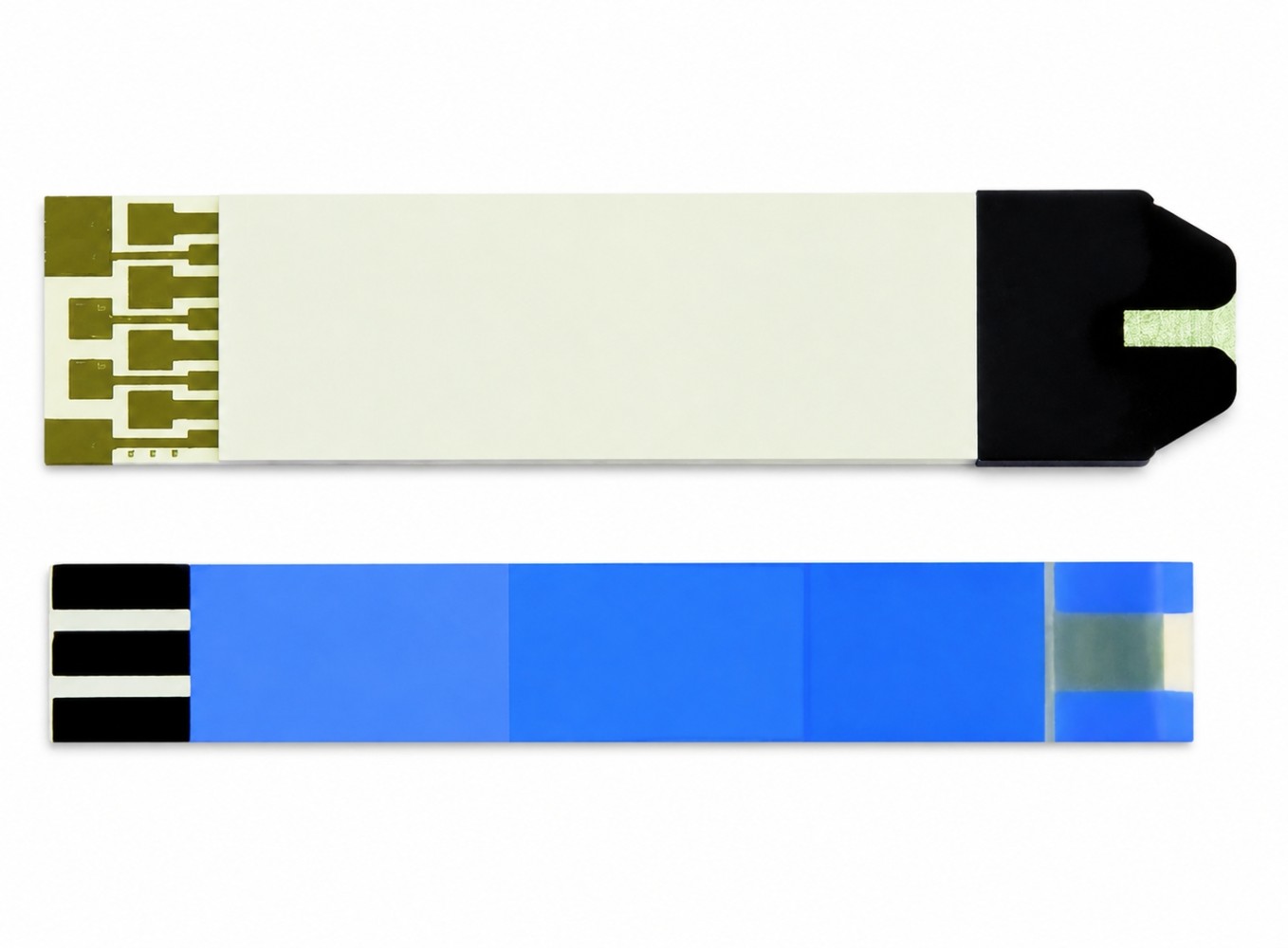
Electrochemical detection of glucose relies on platinum group metal electrodes — screen-printed onto ceramic and fired — that catalyze the reaction between glucose oxidase and hydrogen peroxide. The platinum or Pt/Ag electrode provides electrochemical activity and reproducible sensitivity over many measurement cycles; the ceramic substrate contributes chemical inertness, dimensional stability, and zero moisture uptake. This combination has been in commercial use in clinical glucose analyzers and point-of-care devices for decades.
Our ceramic sensors and thick film microcircuits with Au, Pt/Au, and AgPd metallization are directly applicable here. Electrode geometry, resistor networks for signal conditioning, and hermetic via routing can all be integrated on a single ceramic PCB. The same platform extends to lactate sensors, ion-selective biosensors, and other electrochemical diagnostic devices.
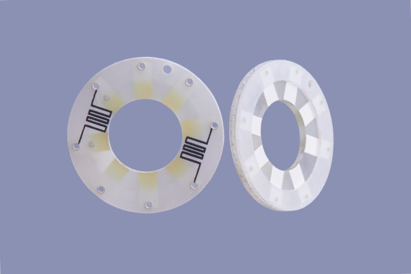
Ultrasound transducer array electronics operate at 1–15 MHz and require substrates with low dielectric loss (Df < 0.001) and dimensional accuracy tight enough to maintain element pitch across the array. A typical design uses 99.6% alumina with gold metallization providing the combination of surface quality and dimensional stability that transducer signal integrity demands.
Intraoral dental X-ray sensor modules face a different constraint: maximum integration density in a very small form factor, with BGA-compatible pad layouts and low-resistance hermetic via construction. High-density multilayer thick film ceramic circuits — up to 8 conductor layers with solid-fill vias and castellated edge metallization — are the established substrate approach for these modules.
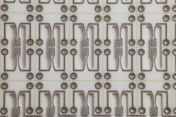
Non-invasive monitoring of blood oxygen and tissue properties commonly uses LED source and photodetector assemblies built on ceramic substrates with hermetic plugged vias and multilayer conductor routing. A SpO₂ sensor module on ceramic integrates LED drive circuitry, detector interface, and signal conditioning in a compact, hermetically constructed assembly stable over the device lifetime. Tissue measurement devices follow a similar architecture: paired SMT ceramic circuits — source and detector — with solid metal-plugged vias and castellated edge metallization for surface-mount attachment.
Our thick film microcircuits and custom hybrid micromodules address this architecture directly, with TO-style window lid compatibility for the optical path where needed.
Alumina is the standard substrate for active implantable electronics for several concurrent reasons: mechanical strength, electrochemical inertness in body fluids, zero water uptake, and RF transparency — which allows telemetry antenna structures to be integrated within the hermetic ceramic housing rather than requiring additional feedthroughs. Leading implantable device manufacturers have long used multilayer ceramic enclosure designs where the hybrid circuit mounts directly onto the ceramic housing, with vias connecting the layers.
Thin film sputtered platinum on polished alumina — is the validated approach for electrode structures and signal routing in implantable circuits, with long-term stability proven in body-temperature environments.
Our thin film microcircuits and DBC substrates on AlN and Si₃N₄, combined with hybrid assembly capabilities including die attach and wire bonding, and precision ceramic processing — laser drilling, cavity machining, and surface finishing — directly support this application space.
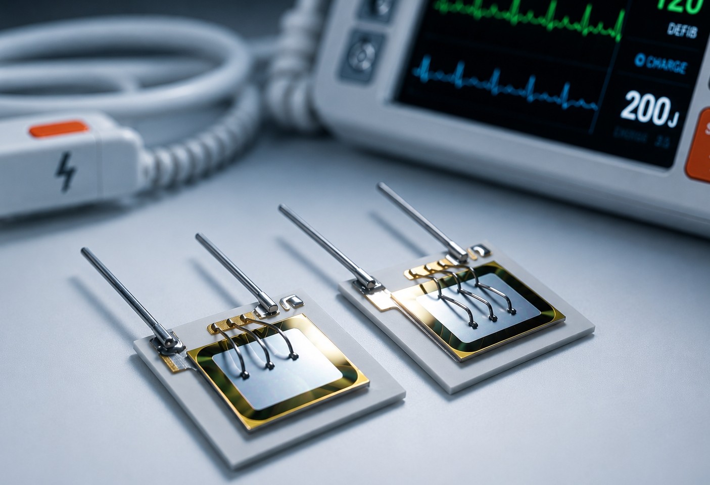
Defibrillator electronics must handle high-voltage charging, energy steering, and discharge control reliably after potentially years of standby. The high-voltage section requires stable dielectric isolation, spike-resistant thick film resistors trimmed to tight tolerances, and a substrate that handles brief but intense thermal transients from discharge events.
Voltage isolation requirements in medical electrical equipment directly shape substrate thickness, metallization geometry, and layout — making early design review an important part of getting these circuits right.
Our DBC substrates and custom power assemblies are the starting point for compact, high-energy medical modules.
Electrosurgical generators deliver 200–400 W of RF power at 300–500 kHz into tissue — a demanding environment for the substrate carrying the power stage. Thick film Ag-Pd conductors on 96% alumina with integrated thick film resistors are the standard approach: good voltage isolation above 5 kV, thermal stability under continuous high-power operation, and proven compatibility with the demanding qualification requirements of surgical equipment.
High-power laser surgical systems — diode-pumped cutting and ablation lasers — present a similar thermal challenge at the die level. AlN substrates with thin film or DBC metallization provide the thermal conductivity needed to keep laser diode junctions within operating spec under continuous duty.
Portable and bedside monitoring equipment — ECG recorders, multi-parameter monitors, infusion pump controllers — requires precision analog electronics stable over the device service life and through clinical cleaning and disinfection cycles. Thick film microcircuits with integrated resistor networks, multilayer conductor structures, and Au or Pt/Au metallization for wire bonding and soldering are well suited here. For sample preparation and temperature-controlled diagnostic processes, our microheaters on alumina and AlN provide precise, stable heating elements on the same ceramic platform. Where the measurement chain demands the highest resistor accuracy, thin film laser-trimmed to ±0.1% delivers it.
India's medical device sector is growing rapidly, and the push toward domestic development of diagnostic, monitoring, and therapeutic equipment is accelerating. Most of the ceramic microcircuit capability these programs require has historically been sourced overseas — with the lead times, minimum order constraints, and communication overhead that entails.
We are in New Delhi, working within the same market, the same regulatory environment, and the same program timelines as our customers. For engineering teams: we review drawings early, flag manufacturability issues, and suggest modifications that improve reliability or reduce cost. For procurement: competitive pricing, flexible minimum quantities, and accessible technical support.
Get a quote or reach out to discuss your application directly.




Strategic Electronics Summit · BIEC, Bengaluru
Book a slot to speak with our engineers at the booth.
