
Company




Proud ELCINA Member
Electronic Industries Association of India
 Ceramic Processing
Laser processing, diamond dicing, lapping and polishing shape ceramic substrates across a wide range of materials.
Ceramic Processing
Laser processing, diamond dicing, lapping and polishing shape ceramic substrates across a wide range of materials.
 Ceramic Metallization
Thick film, thin film, Direct Bonded Copper, and plating processes add functional layers to ceramic.
Ceramic Metallization
Thick film, thin film, Direct Bonded Copper, and plating processes add functional layers to ceramic.
 Hybrid Assembly
Die attach, wire bonding, and sealing turn processed, metallized ceramic into a complete, functional part.
Custom Glass, Paste & Material Development
An in-house capability that supports several of our processes: we synthesize technical glasses and thick-film pastes, and build MEMS structures.
Hybrid Assembly
Die attach, wire bonding, and sealing turn processed, metallized ceramic into a complete, functional part.
Custom Glass, Paste & Material Development
An in-house capability that supports several of our processes: we synthesize technical glasses and thick-film pastes, and build MEMS structures.
Not every product needs to go through the same steps. Some parts are delivered as processed ceramic only — cut, drilled, or shaped to a design, with no metallization or assembly involved. Others are metallized substrates, ready for a customer to assemble on their own line. Others go all the way through assembly and testing, arriving as a complete, finished part. Where a design does call for more than one step, ceramic processing usually comes first, metallization next, and assembly last — though even that order can vary, since a substrate is sometimes cut or trimmed again by laser after it has already been metallized.
Our custom glass and material development work supports these processes without being fixed to one place in the sequence.
Ceramic processing shapes the substrate before or after metallization, depending on the process used, and is applied across a wide range of materials — 96% and 99.6% Al₂O₃, aluminum nitride, silicon nitride, and many others.
Laser processing covers cutting, drilling, scribing, ablation, and marking. Because there is no physical contact with the material, chipping is kept to a minimum and tolerances stay tight and repeatable. This makes it a good choice for complex 2D shapes, small holes, and separating individual parts from a larger panel.
Diamond dicing and profiling create straight cuts, slots, and closely spaced arrays of parts, with clean edges and no chipping. The process works just as well for a few prototypes as it does for a full production run.
Substrates are lapped and polished to a controlled thickness and surface finish. Surface preparation at this stage affects film adhesion, resistor consistency, and how sharply features are defined in the metallization steps that follow.
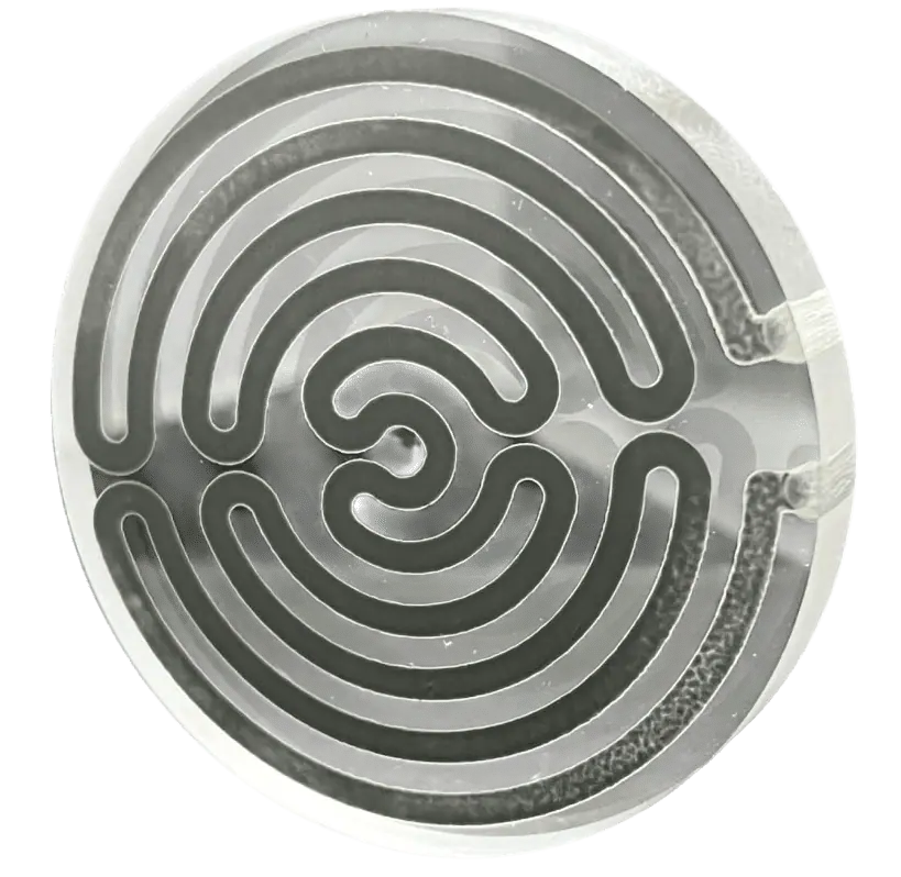
Metallization adds a functional layer to processed ceramic. Depending on the design, this can form a complete electrical circuit, a solderable pad or electrode, a wire-bonding surface, or another function specific to the application. Some form of it is used in most of what we make, including ceramic PCBs, microheaters, sensors, thick and thin film microcircuits, DBC substrates, and the hybrid assemblies built from them.
Conductive pastes (Ag, AgPd, AgPt, Au, Ru, Pt), resistor and thermistor pastes (Ru, RuPdAg, Pt), and glass coatings are screen-printed onto the ceramic and fired to build up multilayer circuits. It is a cost-effective and versatile metallization option, and it supports printed resistors that can be laser-trimmed for close tolerance.
Metal and resistive layers — Cr, V, Ti, NiCr, Ni, Nb, Cu, Al, Au, Pt, and silicon alloys — are deposited under vacuum and patterned using photolithography. This route achieves finer conductor lines, tighter resistor tolerances, and specific layer or metal combinations that screen printing can't reach. We turn to thin film wherever a design calls for that level of precision or a particular layer stack; RF and microwave circuits are a common example, though many RF and microwave designs are also made successfully in thick film.
A layer of oxygen-free copper foil is bonded directly to the ceramic for designs that need to carry high current. Patterning is typically done by chemical etching; laser etching is available as an option where a design needs very fine or highly precise features.
Finish plating (Ni, Au, ENIG, ENIPIG, Ag) and solder masking are applied over thick film, thin film, or DBC. This gives a surface that can be soldered, wire-bonded, and resists corrosion.
Assembly is where processed, metallized ceramic becomes a complete, functional part. It adds the most value per unit, even though it makes up a smaller share of our total output than processing or metallization.
Die, including SiC and GaN devices, are mounted using epoxy or solder. The choice depends on the thermal budget and reliability the design requires.
Aluminum, gold, or platinum wire is bonded by ultrasonic or thermocompression methods to complete the electrical connections between die, substrate, and package.
Assemblies are sealed with epoxy, solder, glass, or laser welding. Before they leave our facility, they are tested electrically and checked for thermal cycling, vibration, and hermeticity.
This is an in-house materials capability behind several of our processes — our thick-film pastes and ceramic-to-ceramic bonding glasses among them.
We synthesize, test, and manufacture our own technical glasses and thick-film pastes, including formulations with no direct commercial equivalent. This lets us adjust a formulation for a specific substrate, temperature range, or reliability target without waiting on a supplier's product roadmap. The same team also has the expertise to develop thermally conductive formulations for thermal interface applications where a standard material falls short of what a design needs.
For gas sensing applications, we build custom MEMS structures directly on ceramic substrates. This combines a tailored substrate and a functional sensing element in a single part.
Specifications like tolerance, resistor stability, and current rating tell you what a process can do. They do not explain why our results stay consistent. Processing, metallization, assembly, and material development are all managed by one engineering team in the same facility. A design change is understood directly by the people who make it happen, without being explained again to an outside supplier. This gives us closer control over the factors that determine reliability — adhesion, CTE matching, resistor drift — and the freedom to adjust a process or a paste formulation to fit your design.
There is rarely one single right answer. Frequency, power, temperature, precision, and cost must often be balanced against each other, and the best result usually comes from combining more than one process. These recommendations are based on how each process performs in real applications, not only on datasheet numbers.
The default choice for cost-sensitive, multilayer, or power-tolerant designs.
Used wherever conductor geometry and resistor precision matter more than cost.
Used when a design must carry high current without excessive resistive loss.
Laser processing works well for complex 2D shapes and small holes; diamond dicing suits straight, closely spaced cuts.
The earlier you bring us into a project, the more useful this becomes. Reaching out while a design is still taking shape lets our engineering team suggest a technology combination that meets your technical requirements and keeps the project cost-effective, rather than working around choices that have already been locked in.
These technologies are used with a wide range of ceramic materials, including cost-effective 96% and 99.6% alumina, aluminum nitride, silicon nitride, zirconia-based ceramics, fused silica, ferrite, and other specialty materials — plus the technical glasses we formulate ourselves for dielectric layers and ceramic-to-ceramic bonding. The right material depends on your thermal, electrical, and mechanical targets. See the full range on our Materials page, or ask our engineering team for a recommendation.
The market offers many different solutions, from large-volume standard parts to specialized custom work. Our position comes from combining ceramic processing, metallization, assembly, and our own materials development within one engineering team, which lets us take on designs that a standardized producer might decline, or would only accept after a lengthy and costly tooling and qualification process. An unusual geometry, a non-standard material combination, or a request outside a fixed process menu is a normal starting point for us, not an exception. Our team has direct experience across automotive, aerospace, defense, semiconductor, and industrial electronics, and our manufacturing base lets us offer customers around the world a fast, cost-competitive path from a first prototype to volume production.
Metallization adds a functional metal layer to a ceramic substrate. Depending on the design, this can form a complete electrical circuit, a solderable pad or electrode, a wire-bonding surface, or another function specific to the application. Most of what we build — PCBs, sensors, microheaters, microcircuits — depends on it in some form, which is why it sits at the center of our process, between ceramic processing and final assembly.
Thick film uses screen-printed pastes that are fired onto the ceramic. It's cost-effective, works well for multilayer circuits, and supports printed resistors. Thin film uses vacuum deposition and photolithography instead, producing finer conductor lines, tighter resistor tolerances, and specific layer or metal combinations that screen printing can't reach. We use thin film wherever a design needs that level of precision or a particular layer stack — RF and microwave circuits are a common example, though many RF and microwave designs are made successfully in thick film too.
Our most commonly used substrate materials are 96% alumina, 99.6% alumina, and aluminum nitride (AlN). We're not limited to these — depending on your application, we can also offer other ceramics such as quartz, zirconia, silicon nitride, and others. If you have a specific material in mind, let's discuss it. You'll find a list of our typical materials on our Materials page.
Yes. Double-sided metallization, with a patterned top layer and a continuous bottom layer, is a standard option. For thin film, our typical stack is a 0.1 µm chromium adhesion layer, followed by 3–10 µm of copper, with an electroless or electroplated Ni, Au, or Ni/Au finish. Other stacks and finishes are available — see the Specifications section of our Thin Film Microcircuits page for the full deposition materials table. Thick film metallization is also worth considering for many applications and can offer real advantages depending on the design.
Our standard capability is 50/50 µm for conductor width and spacing. Finer geometries may be possible depending on the specific design and production volume.
Yes — we can provide gold-finished landing pads suitable for subsequent flip-chip assembly.
For thin film, we generally manufacture double-layer metallization, with through-holes, edge interconnections, and vias as standard capabilities. Circuits with more layers are typically made using our thick film process instead. The most suitable approach depends on your technical requirements — we're happy to go through the options once we understand your design.
Both, depending on the case — but a significant part of our thick-film pastes and the glass systems we use for dielectric layers and ceramic-to-ceramic bonding are synthesized, tested, and manufactured by our own materials team. Some of these formulations have no direct commercial equivalent. Developing them ourselves means we can adjust a formulation for a specific substrate, temperature range, or reliability target without waiting on a supplier's product roadmap.
When the design needs to carry significant current without excessive resistive loss. This is typical of power modules built with IGBT, MOSFET, or SiC devices, where thick film or thin film conductor layers are not thick enough.
Laser processing typically holds positioning accuracy around ±0.05 mm, or ±0.025 mm where a design calls for tighter control. Diamond dicing offers comparable precision with clean, chip-free edges, and performs consistently whether we're cutting one prototype or a full production run.
Please send us your design and any relevant technical requirements — this lets us give specific technical feedback and recommend the most suitable manufacturing approach. It also helps to know the expected quantity. If this is a funded research project, sharing what you can about the anticipated budget, particularly for a one-time prototype run, helps us shape the most cost-effective technical solution and manufacturing route.
Submit Your Request
Please fill out the form and provide as much detail as possible. The more information you share, the more efficient our response will be.
Review & Clarification
We carefully review your specifications and may contact you for clarification. We provide as much cooperation and communication as your project requires.
Tailored Quotation
You will receive a competitive offer including pricing, estimated lead times, technical details, and, if relevant, alternative solutions.
Ongoing Support
After confirmation, we stay with you throughout production, delivery, and product use — ensuring reliable service and long-term cooperation.




Strategic Electronics Summit · BIEC, Bengaluru
Book a slot to speak with our engineers at the booth.
